- 您现在的位置:买卖IC网 > Sheet目录444 > IRF7526D1PBF (International Rectifier)MOSFET P-CH 30V 2A MICRO8
�� �
�
�PD� -95437�
�IRF7526D1PbF�
�l�
�Co-packaged� HEXFET� ?� Power�
�MOSFET� and� Schottky� Diode�
�FETKY� TM� MOSFET� &� Schottky� Diode�
�l�
�l�
�l�
�l�
�l�
�P-Channel� HEXFET�
�Low� V� F� Schottky� Rectifier�
�Generation� 5� Technology�
�Micro8� TM� Footprint�
�Lead-Free�
�A�
�A�
�S�
�G�
�1�
�2�
�3�
�4�
�8�
�7�
�6�
�5�
�K�
�K�
�D�
�D�
�V� DSS� =� -30V�
�R� DS(on)� =� 0.20� ?�
�Schottky� Vf� =� 0.39V�
�Description�
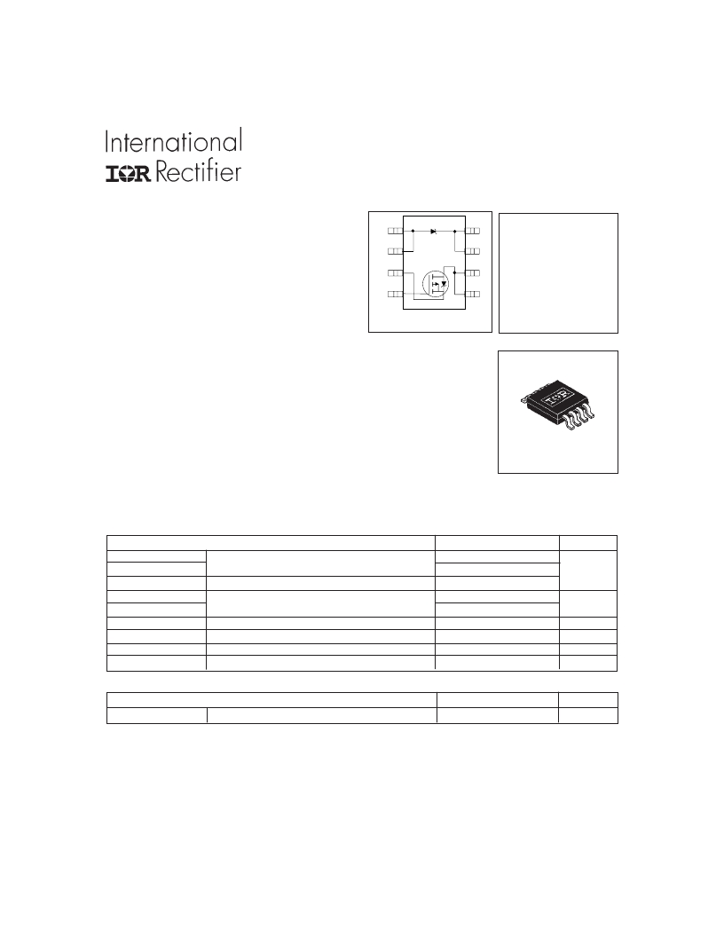
�Top� View�
�The� FETKY�
�TM�
�family� of� co-packaged� HEXFETs� and� Schottky� diodes� offer� the�
�designer� an� innovative� board� space� saving� solution� for� switching� regulator�
�applications.� Generation� 5� HEXFETs� utilize� advanced� processing� techniques� to�
�achieve� extremely� low� on-resistance� per� silicon� area.� Combining� this� technology�
�with� International� Rectifier's� low� forward� drop� Schottky� rectifiers� results� in� an�
�extremely� efficient� device� suitable� for� use� in� a� wide� variety� of� portable� electronics�
�applications� like� cell� phone,� PDA,� etc.�
�The� new� Micro8� package,� with� half� the� footprint� area� of� the� standard� SO-8,� provides�
�the� smallest� footprint� available� in� an� SOIC� outline.� This� makes� the� Micro8�
�an� ideal�
�profile� (<1.1mm)� of� the� Micro8�
�will� allow� it� to� fit� easily� into� extremely� thin� application�
�TM�
�TM�
�device� for� applications� where� printed� circuit� board� space� is� at� a� premium.� The� low�
�TM�
�environments� such� as� portable� electronics� and� PCMCIA� cards.�
�Absolute� Maximum� Ratings�
�Micro8�
�TM�
�Parameter�
�Maximum�
�Units�
�I� D� @� T� A� =� 25°C�
�I� D� @� T� A� =� 70°C�
�I� DM�
�P� D� @T� A� =� 25°C�
�P� D� @T� A� =� 70°C�
�V� GS�
�dv/dt�
�T� J,� T� STG�
�Continuous� Drain� Current,� V� GS� @� -4.5V�
�Pulsed� Drain� Current� à�
�Power� Dissipation�
�Linear� Derating� Factor�
�Gate-to-Source� Voltage�
�Peak� Diode� Recovery� dv/dt� á�
�Junction� and� Storage� Temperature� Range�
�-2.0�
�-1.6�
�-16�
�1.25�
�0.8�
�10�
�±� 20�
�-5.0�
�-55� to� +150�
�A�
�W�
�mW/°C�
�V�
�V/ns�
�°C�
�Thermal� Resistance� Ratings�
�Parameter�
�Maximum�
�Units�
�R� θ� JA�
�Junction-to-Ambient� ?�
�100�
�°C/W�
�Notes:�
�?� Repetitive� rating� –� pulse� width� limited� by� max.� junction� temperature� (see� Fig.� 9)�
�?� I� SD� ≤� -1.2A,� di/dt� ≤� 160A/μs,� V� DD� ≤� V� (BR)DSS� ,� T� J� ≤� 150°C�
�?� Pulse� width� ≤� 300μs� –� duty� cycle� ≤� 2%�
�?� When� mounted� on� 1� inch� square� copper� board� to� approximate� typical� multi-layer� PCB� thermal� resistance�
�www.irf.com�
�1�
�02/22/05�
�发布紧急采购,3分钟左右您将得到回复。
相关PDF资料
IRF7526D1TR
MOSFET P-CH 30V 2A MICRO8
IRF7601TR
MOSFET N-CH 20V 5.7A MICRO8
IRF7603TR
MOSFET N-CH 30V 5.6A MICRO8
IRF7604TRPBF
MOSFET P-CH 20V 3.6A MICRO8
IRF7604TR
MOSFET P-CH 20V 3.6A MICRO8
IRF7607
MOSFET N-CH 20V 6.5A MICRO-8
IRF7663TR
MOSFET P-CH 20V 8.2A MICRO8
IRF7700GTRPBF
MOSFET P-CH 20V 8.6A 8-TSSOP
相关代理商/技术参数
IRF7526D1TR
功能描述:MOSFET P-CH 30V 2A MICRO8 RoHS:否 类别:分离式半导体产品 >> FET - 单 系列:FETKY™ 标准包装:1,000 系列:MESH OVERLAY™ FET 型:MOSFET N 通道,金属氧化物 FET 特点:逻辑电平门 漏极至源极电压(Vdss):200V 电流 - 连续漏极(Id) @ 25° C:18A 开态Rds(最大)@ Id, Vgs @ 25° C:180 毫欧 @ 9A,10V Id 时的 Vgs(th)(最大):4V @ 250µA 闸电荷(Qg) @ Vgs:72nC @ 10V 输入电容 (Ciss) @ Vds:1560pF @ 25V 功率 - 最大:40W 安装类型:通孔 封装/外壳:TO-220-3 整包 供应商设备封装:TO-220FP 包装:管件
IRF7526D1TRPBF
功能描述:MOSFET MOSFT PCh w/Schttky -2A 200mOhm 7.5nC RoHS:否 制造商:STMicroelectronics 晶体管极性:N-Channel 汲极/源极击穿电压:650 V 闸/源击穿电压:25 V 漏极连续电流:130 A 电阻汲极/源极 RDS(导通):0.014 Ohms 配置:Single 最大工作温度: 安装风格:Through Hole 封装 / 箱体:Max247 封装:Tube
IRF7530
制造商:IRF 制造商全称:International Rectifier 功能描述:Power MOSFET(Vdss=20V, Rds(on)=0.030ohm)
IRF7530PBF
功能描述:MOSFET RoHS:否 制造商:STMicroelectronics 晶体管极性:N-Channel 汲极/源极击穿电压:650 V 闸/源击穿电压:25 V 漏极连续电流:130 A 电阻汲极/源极 RDS(导通):0.014 Ohms 配置:Single 最大工作温度: 安装风格:Through Hole 封装 / 箱体:Max247 封装:Tube
IRF7530PBF
制造商:International Rectifier 功能描述:MOSFET
IRF7530TR
功能描述:MOSFET 2N-CH 20V 5.4A MICRO8 RoHS:否 类别:分离式半导体产品 >> FET - 阵列 系列:HEXFET® 产品目录绘图:8-SOIC Mosfet Package 标准包装:1 系列:- FET 型:2 个 N 沟道(双) FET 特点:逻辑电平门 漏极至源极电压(Vdss):60V 电流 - 连续漏极(Id) @ 25° C:3A 开态Rds(最大)@ Id, Vgs @ 25° C:75 毫欧 @ 4.6A,10V Id 时的 Vgs(th)(最大):3V @ 250µA 闸电荷(Qg) @ Vgs:20nC @ 10V 输入电容 (Ciss) @ Vds:- 功率 - 最大:1.4W 安装类型:表面贴装 封装/外壳:PowerPAK? SO-8 供应商设备封装:PowerPAK? SO-8 包装:Digi-Reel® 产品目录页面:1664 (CN2011-ZH PDF) 其它名称:SI7948DP-T1-GE3DKR
IRF7530TRPBF
功能描述:MOSFET MOSFT DUAL NCh 20V 5.4A Micro 8 RoHS:否 制造商:STMicroelectronics 晶体管极性:N-Channel 汲极/源极击穿电压:650 V 闸/源击穿电压:25 V 漏极连续电流:130 A 电阻汲极/源极 RDS(导通):0.014 Ohms 配置:Single 最大工作温度: 安装风格:Through Hole 封装 / 箱体:Max247 封装:Tube
IRF7530TRPBF-EL
制造商:International Rectifier 功能描述: